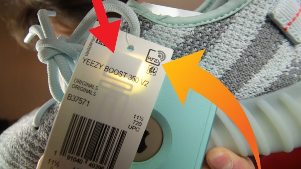
Today, RFID technology has entered all walks of life, exerting powerful digital collection capabilities in different application scenarios and links. However, in practical applications, label identification often encounters various challenges, including not only environmental factors, but also product technology and so on. For manufacturers who use RFID systems, easy-to-use RFID labels are a key to the success of the project.
Objectively speaking, an easy-to-use RFID label contains many elements, such as excellent performance, strong storage capacity and environmental adaptability, as well as an aesthetically pleasing antenna design, an irresistible price, etc.
From the perspective of RFID label manufacturing, the processing methods of each link including chip, antenna design, binding, compounding, and packaging will have an impact on the final finished label. In this process, not only must the performance of the RFID tag be guaranteed, but also the consistency of the tag must be ensured. Therefore, even the top RFID label manufacturers cannot guarantee that the labels they produce are “safe.”
In a label processing process, INLAY is usually used as a “sandwich layer” composite material. INLAY enters the compound processing production link as a material, so it must be affected by the five elements of compound personnel, processing equipment, materials, technology, and processing environment.
For example, when a customer proposes to attach an RFID label to metal, it shows that he needs an anti-metal tag. However, this is far from enough. We also need to know more about what material is the metal surface to be pasted on? What kind of dielectric is it? What is the thickness and size of the metal surface? And, what kind of effect the final RFID tag needs to achieve, and so on.
In the footwear and apparel industry, customers may require large quantities of electronic tag, and will require the surface treatment of the electronic tag, the processor may directly perform bronzing treatment on the surface, or use other processes. In this link, the material used for bronzing is also metal. You need to know whether you are using a cold stamping or hot stamping process, what kind of dielectric is used, what kind of material, including the bronzing area, and so on.
In the process of chip processing, many details will be finalized. Some chips are very sensitive to bonding, and slight deviations in the position and direction of chip bonding will have a significant impact on electrical performance. The PET aluminum etched antenna will generate volatile gas when heated. In the binding process, the heating is heating and curing. Since the conductive glue has been covered on the antenna, air bubbles may be generated, which will definitely affect the performance.
When we start from the needs and approach the label processing technology step by step, we are getting closer and closer to the essence of a good label, which is composed of countless specific and subtle details. As a result, we can also more truly realize that a good label needs to gather the experience of the entire industry chain and the hard work of countless practitioners.


